Dry etching vs. wet etching
Etching is a fundamental, simple, and very old technique in which material is removed from a surface by corrosive action.
Whereas Etching was first used to engrave copper centuries ago, it is now frequently in use to prepare printed circuit boards. In reality, without the contemporary wet and dry etching procedures employed in electronic device manufacture, today’s microelectronics industry would be almost non-existent.
Generally, you will find two types of etching techniques: Wet Etching is when the material is submerged in a chemical solution and dissolves.
Dry Etching involves sputtering or dissolving the material with reactive ions or a vapor phase etchant.
Wet Etching
This is a kind of method which involves immersing wafers in a chemical bath and etching silicon dioxide onto a silicon substrate with etchants such as hydrofluoric acid.
Keep in mind it is the most basic etching method, although considered less accurate than dry Etching, and creates poisonous waste that must be carefully disposed of.
Many wet engravers are demanding about the materials they deal with.
Wet Etching is commonly used due to one factor, known selectivity.
High selectivity allows for the use of smaller masks and the ability to suddenly stop etching on the layer beneath the layer being etched.
Unfortunately, there are issues since a mask is usually employed to etch the material selectively.
This needs the use of a mask that does not dissolve or, at the very least, etches significantly more than usual.
Dry Etching
On the other hand, Dry Etching is a plasma-based procedure that uses gas mixes to induce a reaction that affects the wafer surface.
Radio waves excite gas molecules and modify their states, resulting in a chemical process that eradicates undesired material and leaves an etched surface.
The dry etching technique is divided into three main categories:
- Vapour phase etching
- Sputter etching
- Etching using reactive ions (RIE)
Depending on the plasma settings working, the etchings created with plasma can differ.
Typical plasma etching uses a pressure range of 0.1 to 5 Torr (about 133.3 Pa). Plasma generates energetic, neutrally charged free radicals, which react on the wafer surface.
This is the isotropic method because the neutral particles hit the wafer from all sides.
Instead, oxygen plasma will be used to oxidize the photoresist and make it easier to remove.
The plasma gas is usually comprised of chlorine or fluorine-rich molecules. Carbon tetrachloride (CCl4), for example, has been known to attack silicon and aluminum, whereas trifluoromethane has been known to target silicon dioxide and silicon nitride.
Lon milling
It is another extensively used technology. This method, also known as sputter etching, employs lower pressures of roughly 10-4 Torr (10 mPa).
It involves blasting the wafer with energetic ions of noble gases such as Ar+, which transmit kinetic energy and drop the atoms off the substrate.
This method is anisotropic since the Etching is done by bombarding the wafer with ions in a single direction. This process still has poor selectivity.
The well-known reactive ion etching technique (RIE for Reactive Ion Etching) operates halfway between sputtering and plasma etching (between 10-3 and 10-1 Torr). It is a kind of reactive ion etching that produces deeper and narrower features than RIE.


Range
Wet and dry Etching equally involves removing layers from a masked surface to enable three-dimensional nanostructure transfer in a variety of applications, including microelectronics, photonics, and medicine.
Which one is best for your application is determined by a number of factors.
The main differences
In the end, you can see that we have discussed different etching procedures thoroughly.
Dry and wet etchings are the two most common etching processes for removing surface materials and generating patterns on surfaces.
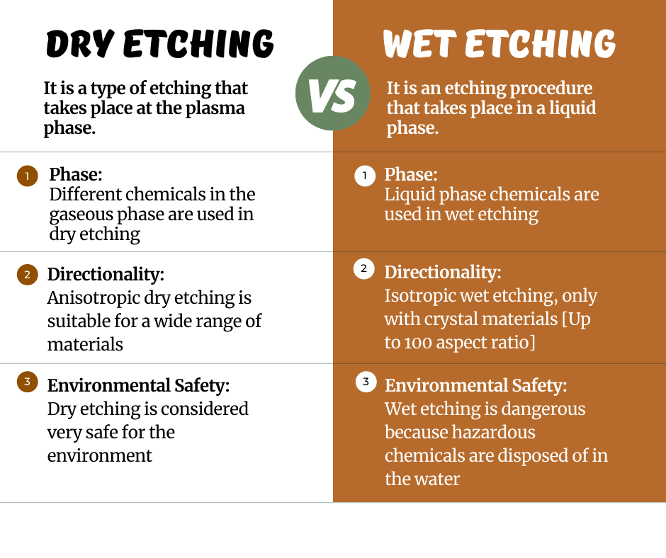
The difference between wet and dry Etching is that wet Etching uses liquid chemicals or etching agents, whereas dry Etching uses plasmas or etching gases.
In the production of microelectronic components, Etching is considered a key process.